How to make a PCB, easy and cheap – at home
PCB = Printed Circuit Board (for who doesn’t know yet)
Since I had to design and develop different testing electronic circuits it was also necessary to create their PCBs. One solution was to print on a paper the PCB and go to a company from the town which to copy from the paper to the cooper board. This solution sounds really easy but there are some major disadvantages: the quality of cooper printing is not so good, it become quite expensive when it is necessary to create many different versions of a PCB and it is not possible to create a double side circuit (they doesn’t know how to align them ad I’m sure that they wouldn’t have time for me to explain them). On Internet could be found different companies which print PCB on copper boards, even double sided, but the price is really high when it is about just a prototype board. The remaining solution was to print the PCB drawing and to make the transfer to the cooper board on my own.
In previous work I have used Cadence Orcad software application for creating the electronic circuit schematics. Even so, I’m quite new in this domain. I decided to take a look and analyze a set of software applications necessary for accomplish this goal and finally I decided to use Proteus PCB Design Software. It permits to create the circuit schematic, to run simulations, to create very easy new components (including footprint), if they are not included into the library, and to realize the associated PCB (it includes an auto-route function).
Necessary materials:
- photo paper / some paper from a magazine
- cooper board
- a laser printer
- household iron
- ferric chloride
- scotch
Steps to create the PCB, easy and cheap:
:: Create the schematic and design using any dedicated software application
For Proteus PCB Design Software there are a lot of simple and easy understandable tutorials on youtube. I use this source and give results very quickly. After you are sure that the schematic is correct and all components were added on the PCB layout go to the next step.
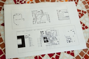
:: Print the PCB on a photo paper
I found to be 2 posibilities as paper which to be used for printing: using special unused photo paper or using some paper from old magazines, which you don’t need anymore. I have tested only the first possibility. It is very important to verify that your printer supports that type of paper (for not producing damages to the printer). Also, it is necessary that the printer to be a laser printer. The special ink of this type of printer supports warm transfer and resist to ferric chloride.
It is important that the PCB to be printed at 100% scale. So, verify the scale before printing (in Print dialog and Properties). I made first some tests by printing on normal simple papers and when I get what I want I print on the photo paper.
Take in consideration that the PCB will appear mirrored on the copper board. In my case I had to create the board to be double-sided. On a side I had SMD (Surface Mount Device) components and on the other side I had normal format electronic components (whit pins goes through holes from one side to another side of the board). I had to print the top side mirrored and the bottom side not mirrored. In this way I will obtain the exact PCB format which I want.
You have also to cut the unnecessary paper around the PCB circuits but leaving a margin of about 0.5 cm. I print also the circuit borders, so it was easy to cut after using a scissors.
:: Prepare the cooper board
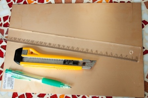
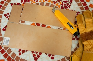
The cooper board have to be cut at the size of the PCB. A margin of 0.5 cm could be leaved around it. For this I have use a pen to draw the shape on the copper board and a cutter to scratch (partially cut) the cooper material, on the paths drawn with the pen. It have to be scratched many times, on the same cutting path, for being sure that the copper material have been completely cut (it also depends on the cooper thickness). Be careful to not cut yourself. It remains the rest of the material (plastic or fiber glass, under the cooper layer) which have to be cut.
You have to use a pair of gloves for bending the board on the line (path) which you have just scratched. If it is bended to a corresponding angle it will break across the line. If you have multiple scrached lines bend them one by one. This operation will permit you to get nice borders and with minimum effort. If you have a double sided cooper board you have to scratch it on both sides across a cutting line.
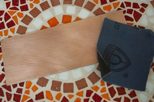
After you cut it to the necessary size you have to clean the cooper surface and prepare it for ink transfer and ferric chloride etching. I have use some sandpaper for eliminating any undesirable substances / materials from the cooper surface and when clean it with some fabric material and alcohol. Clean all the surface and don’t miss any areas. Try to not put your fingerprints on it after.
:: Transfer the ink from paper to cooper board
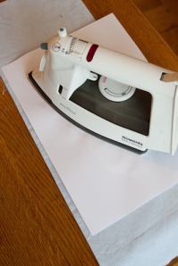
For transferring the PCB to the cooper board the printed photo paper should be put on the cooper board, with the printed side to touch the cooper. The printed paper should be fixed to the cooper board for not moving during the transfer (otherwise the result will not be at all what you expected). For fixing them some scotch could be used. Under the cooper board should be put some material resistant to temperature and on the top of photo paper a sheet of normal paper.
The next step will require a very important and very used in science domain tool: a household iron :D. Warm it to maximum temperature and turn off steam. When it is ready you have to put on top of all and press strong moving back and forward. Do this for about 3-5 minutes. Long time and strong press ensure a good transfer. Be aware that the cooper board will be very hot at the end. Wait for it to cool down.
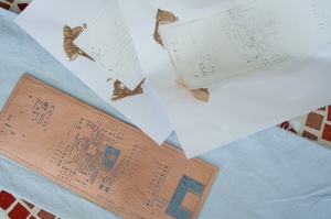
Wash the board with some warm water to remove all the paper from it. Wash until all the paper is gone. Don’t be afraid about the ink, it will remains where it is.
:: Etching process
You have to put the cooper board into ferric chloride and let it stay for about 15-20 minutes. Don’t let it more because the thin circuits could be destroyed (I do this mistake of forgetting it for about half an hour … the necessary time depends on the ferric chloride concentration, temperature). After this period of time verify the etching process to see if it is completed. If it is not complete wait for more. Then you consider that it is finished wash the board with lot of water for remove all trace of ferric chloride substance.
:: Success
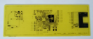
Now you have the PCB created. You have to drill the necessary holes and put the electronic components. Make tests and use your result being proud of your work. 🙂
this is so good..
Please tell me, What is the concetration of ferric chloride in making pcb ?
I just buy the ferric chloride substance from the electronics shop, but I didn’t studied its concentration.